
Hi All,
Just got back the latest version of the Riffle 0.1.1 board, nicely assembled by the kind folks MacroFab.

Alas, when I used an ISP programmer to attempt to load a bootloader -- no dice! Didn't work.
I've been taught by folks that it's usually the case that a 'dead' board design can be brought to life with a few jumper wires ... so, I spent a while using a multimeter to track down the problem, and the main problem seems to be that I made a mistake when wiring up the switch that allows for changing battery chemistries.
The older, working version of the Riffle -- 0.96 -- had a simpler switch configuration:

(The full schematic for version 0.96 is here).
In modifying the board to accommodate two battery chemistries, in version 0.1.1, I think I goofed when assigning pins on the new switch:

(The full schematic for version 0.1.1 is here)
Basically, I misread the switch datasheet re: which pins on the switch would allow for connecting power appropriately. Oops. :( I'm going to go back and reread the datasheet on the switch device -- I might've confused part numbers or something -- but I can also simply do a compare / contrast between the older schematic + board layout and the current one to make sure that things are wired properly.
By properly connecting power across the switch (from VBAT -- which gets power from the USB via the lipo battery charger -- to VDD), I was easily able to load a bootloader:

But, after loading a bootloader, was unable to program the board with a sketch in the Arduino IDE, via USB as per normal. It gave a "avrdude stk500_getsync(): not in sync" error.
However, after playing around with a lot of iterations, I figured out that by connecting a battery to VBAT, I was able to program the board. Alternatively: if, instead of connecting VDD to VBAT, I connected VDD to to VBUS (i.e., directly to USB), I was also able to program the board successfully:

So, in addition to fixing the wiring on the switch (straightforward), there's some more subtle issue re: the power wiring on the board. I'm going to do some more testing with the multimeter tonight, and ask around tomorrow.
Favor -- anyone who has the time, could you check out the power circuitry on the board, and let me know if you see something dumb? :)
Onward!
Cheers, Don
10 Comments
Update -- based on some tinkering, and some great feedback from folks on the plots-waterquality google group:
The power issues no longer seem mysterious. The first, primary issue, as described above, is: I simply wired up the switch improperly, so that power wasn't reaching the microcontroller. That is a simple fix.
The second, more interesting issue has to do with the lithium battery controller chip ("IC2", in the above schematics) on the board. This chip -- the MCP73831 -- is designed to be connected to a power source on its "VIN" pin, and then on its "VBAT" pin, to be connected to both a lithium battery, and to a load. It then does some fancy stuff to manage this power setup -- but it assumes that a battery is connected. If no battery connected, its behavior is likely unpredictable -- it may or may not provide enough current to the load. This is consistent with what I have seen recently, and in previous prototyping of this circuit -- when the battery is not present, but the board was plugged into USB power, sometimes the microcontroller would behave oddly (e.g. not allow for programming via the Arduino IDE).
One simple solution, given the current circuit: always have a battery plugged in. Given the current circuit setup (with appropriate fixes to the arrangement of pins on the switch, so that things are connected properly), this would mean that, in order to program the boards when plugged into USB, we'd always need to have either a lithium battery plugged into the lithium JST port, or some battery plugged into the "general" JST port -- and we'd need to make sure that the switch was in the appropriate position.
This solution 'works' -- but it's less than ideal. Given the way the UNO and most other hobby electronics boards behave, one expects to be able to program the device when power is provided via USB, and it's odd and a bit inconvenient to require a battery being present. Also, the real purpose of the 'switch' has been to provide an 'on-off' functionality on the board, so that one can conserve battery power when the device isn't deployed. Currently (again, with the proper wiring changes), the switch in the circuit effectively decides between the two battery sources ... which means that the effective "on" and "off" positions will be swapped, depending on which battery is plugged in. One must be careful not to plug in more than one battery at once.
All of this is an argument for a more intelligent power circuit.
Brian Mayton yesterday suggested an alternative:
The idea: we can provide the microcontroller (the open rectangle on the far right of the diagram) with power from all three sources -- USB (labeled "USB"), lithium battery (denoted by a battery symbol -- a few horizontal lines), and an alternative battery source "ALT" -- at the same time, and use diodes to select which power source is used. The switch can then be put on the far right of the circuit, so that it truly operates as an "on/off" switch.
Another reason to put diodes in the circuit this way: it protects each of the power sources from being "charged" by the others, if multiple sources are plugged in. This is important, and something I see now should've been done, anyway: for example, if we're going to allow for a 'general chemistry' battery on one of the JST connectors, we would like to protect USB (at 5 V) from being overwhelmed by a >5V battery plugged into that JST connector. A diode serves this function.
So, I'm planning on implementing a new power circuit, as in the above diagram, using diodes as both protection and power management. The only trick is to find diodes that have a relatively low forward voltage drop -- the amount of voltage lost when connecting across it.
Last night I found a discussion of such diodes, here: http://www.electro-tech-online.com/threads/need-1n5817-smt-version-or-equivalent.92710/
With some recommendations:
http://www.vishay.com/docs/88746/ss12.pdf http://www.digikey.com/product-detail/en/BAT54-7-F/BAT54-FDICT-ND/717819 http://www.digikey.com/product-detail/en/CUS08F30,H3F/CUS08F30H3FCT-ND/5114376 https://solarbotics.com/download.php?file=189 http://www.digikey.com/product-detail/en/SM4002PL-TP/SM4002PL-TPMSCT-ND/1793404 http://www.mccsemi.com/up_pdf/SM4001PL-SM4007PL(SOD-123FL).PDF http://www.digikey.com/product-detail/en/SM4002PL-TP/SM4002PL-TPMSCT-ND/1793404
I'm going to sort through the datasheets this morning and see which ones might work best.
Meanwhile, if anyone reading this has better ideas / any additional input, do drop a line! :)
Cheers, Don
Is this a question? Click here to post it to the Questions page.
Reply to this comment...
Log in to comment
Update: I've attempted to incorporate both the fix to the switch, and the new diode-based power management strategy, in the Riffle 0.1.4 schematic. The key part of the schematic is here:
Here's an explanation:
VBUS: connected to 5V from USB
VGEN1: connected a two-pin header on the board (JP1), feeds into the voltage regulator IC4 -- allowing any battery chemistry (under 6V)
VGEN2: connected to a JST connector (CN2), feeds into the voltage regulator IC4 -- allowing any battery chemistry (under 6V)
VBAT: connected to a JST connector (CNL) for a 3.7V Lithium battery, which is charged by VBUS via U1 and also feeds into the voltage regulator IC4
J1: an on/off switch in front of the voltage regulator IC4
IC4: a linear dropout regulator --> can take incoming voltage <=6 Volts, outputs 3.3 volts
VCC: 3.3V, powers the board (including the microcontroller)
U1: the Lithium battery charger
The idea is that the diodes on the parallel VGEN1, VGEN2, VBUS, and VBAT lines -- which all lead into the LDO -- effectively select for the highest-voltage source, and also avoid problems if more than one power source is plugged in at once. (Plugging into USB (VBUS) and having a lithium battery plugged into CNL will result in charging the battery; if no battery is connected to CNL but USB is connected, the board will still receive power.)
Whaddya think?
Is this a question? Click here to post it to the Questions page.
Reply to this comment...
Log in to comment
Update:
What I'd observed was that the previous version of the riffle -- 0.96 -- seemed to allow for USB programming even when a battery wasn't plugged in. (There were a lot of odd parts of the self-assembly process, so I can't be sure that this was always the case ... but recently, for boards that were working, this seems to be mostly true).
In contrast, the latest version of the riffle -- 0.1.1 (yes, the numbering scheme reset -- but nevermind that for now) didn't seem to allow for programming over USB when the battery wasn't present.
It'd be nice not to need a battery when testing / programming the boards.
The initial response on the part of colleagues I've asked -- that this is an instability on the part of the lithium battery charger IC (which is providing all of the current to the Atmel328p) -- seems increasingly likely to be correct.
I found a discussion online -- http://www.microchip.com/forums/m/tm.aspx?m=670010 -- of precisely the same issue, with precisely the same chip. The solution that worked for one of the posters was to place a ~ 10 uF capacitor on the power line connecting the charger chip to the LDO. The thinking is that this capacitor smooths out any power fluctuations between the two chips.
When I examined my schematics and board layouts, I found that on both versions, I have a 10uF capacitor (C5) that is intended to be between the charger chip and the LDO. (I'd copied a schematic from rayshobby.net -- Rui knows what he's doing, but I myself hadn't yet understood the rationale for every capacitor in his schematic:)).
However, on version 0.96, C5 was very close to the LDO (and far away from the charger chip):
In the above picture, I've tried to annotate the relevant chips with ragged white circles. The LDO and C5 are on the right, close together.
.... whereas on version 0.1.1, I'd moved C5 relatively far away from both the charger chip and the LDO:
You can see (if you can parse my annotation) that on 0.1.1, all three parts -- the charger chip, the LDO, and C5 -- are relatively far away from one another on the board.
I'm going to experiment with manually placing a 10uF capacitor on the 0.1.1 version between the power and ground of the LDO, and see whether I can program the board without a battery plugged in.
Additionally, I found a blog post by someone who relied on a a Microchip application note design to build a simple circuit (with the same lithium charging chip that we're using) that handles "load balancing" between USB power and the battery in a more robust way than is possible with the charging chip alone. The design apparently improves the dynamics of battery charging while also solidly enabling programming via USB without a battery present. It only requires two or three extra components, all of which I think I already have elsewhere in my design -- so I'm going to look into making my own version of this design.
So, progress: we have an explanation for the odd behavior, and perhaps we'll find that simply moving a capacitor on the board in the previous 0.1.1 design will allow for USB programming without a battery; and we also have a simple design modification that might make this feature more robust, and allow for improved battery charging.
Is this a question? Click here to post it to the Questions page.
Reply to this comment...
Log in to comment
For further reference (both of the below pics are from the above-referenced blog post, the minimal schematic for the charger chip (which I'd been using) is here:
The load-sharing modification (which I'm studying right now) is here:
Reply to this comment...
Log in to comment
Okay, here's my interpretation of the more advanced circuit:
Full schematic:
Close-up on the relevant power circuitry:
Load balancing is accomplished between USB and the Lithium battery, culminating in the "VDD" line going into a switch. Connecting VDD to the LDO, either USB, the lithium battery, or both can be plugged in, and power to the LDO via LDD will be robust. Also, the dynamics of lithium battery charging will be enhanced (as described in the above-referenced blog post). I need to choose a suitable value of R11 -- it was chosen as 100K in the blog post, but I need to go through the calculation for our case (depends on the characteristics of e.g. the diode we're using as D3, I think).
The switch switches between VDD (USB/Lithium) and VGEN1. VGEN1 connects to two possible power inputs -- a JST connector, or two breakout pins (+, -) on the board. There is currently no diode protection on either -- so it will be important not to plug in a power source into both inputs simultaneously. We might decide to include parallel diodes on these two input lines, so that each source is protected against the other; the downside of doing so would be the associated forward diode voltage drop. It might be nice to leave the diodes off so that folks who want to connect custom power boards that produce a voltage close to 3.3V don't have to deal with the forward voltage drop; and I'm imagining that it's unlikely that people will want to / try to plug in power to both of these sources at once.
... but what do y'all think -- is it better to be fully protected, with diodes?
Is this a question? Click here to post it to the Questions page.
Reply to this comment...
Log in to comment
(Also note: I've added an extra capacitor to the circuit, so that I'll have a 10uF close to the lithium charger, and on both sides of the LDO)
Reply to this comment...
Log in to comment
Further elaboration on this circuit solution:
The idea (nicely described in the blog post) is to use a P-channel Mosfet arranged so that when USB power is applied, this will effectively disconnect the battery from the LDO (while continuing to charge the battery). This also has the effect, apparently, of improving the charging dynamics for the battery. Additionally there's a diode placed on the USB line to avoid the battery charge flowing back to the USB power source.
The P-Mosfet I'm currently using is the FDN340p; the diode is a MBR120VLSFT3G. There are calculations in the blog post to make sure that the gate level on the mosfet is reasonable by dialing in a particular value of a resistor in the circuit (in the blog post, R2; in my schematic, R11). The relevant parameters are about the same for the current leakage of the diode, so the same resistance of 100K for R11 (100K was used for R2) seems reasonable.
The estimated leakage current of battery through the diode (question -- does this happen when USB is disconnected?) is 150 uA. This might be something like 10X the current drawn by the 328p when it's asleep, I think.
However: I further modified the switch circuitry so that it decides between the USB/Lithium circuitry, and a single "VGEN1" power line, which is alternatively supplied by plugging in a power source to a JST connector, or two pins broken out directly on the board. For now, I'm opting to not place diodes on either of the two power sources going into the VGEN1. The idea is that if someone wants to really maximize their battery life, they can plug their battery (alkaline or lithium) into one of the VGEN1 connectors. We'll have to hope that they avoid plugging a battery into both VGEN1 lines; but I'm thinking that the risk of this isn't great.
So, I'm liking this circuit: it maximizes charging dynamics; the lithium battery performs reasonably well (modulo battery leakage through a diode) when plugged into the same circuit that can charge it; but if you really want to maximize battery life with the same lithium battery, you can plug it into VEGEN1 on the board, which has no associated diode. And of course, one can use whatever power source (between 6V and 3.5V, determined by the LDO parameters) one likes on VGEN1.
Is this a question? Click here to post it to the Questions page.
Reply to this comment...
Log in to comment
Hey All!
Okay, after a bunch of discussion last night, it seems that the above P-Mos circuit will work, but the battery leakage is significant. And anyway, having diodes on the input lines is a good idea, in that it automatically selects the highest-voltage power input, and also protects folks again accidentally plugging the battery in the wrong way.
So I've implemented a new version of the design that reverts back to diode-based power selection. But I've also added solder jumpers on the input lines, so one can get around the diodes, if one wishes. So: best of both worlds :)
Finally, I've added another solder jumper + cuttable trace combo so that one can bypass the LDO directly. This allows one to power the 328p and the rest of the board directly with two AA alkaline batteries, and avoids any power drainage from the LDO. This might be a nice option for some folks to really get maximum longevity in the field. You can see the cuttable trace ("T1") here:
I've wrapped up a board design (0.1.7.1) that incoporates these elements, here:
https://github.com/OpenWaterProject/riffle/blob/master/hardware/riffle-beta-0.1.0/riffle-beta-0.1.7.1-board.png https://github.com/OpenWaterProject/riffle/blob/master/hardware/riffle-beta-0.1.0/riffle-beta-0.1.7.1-schem.png
Here's a close-up of the latest power (0.1.7.1) circuit:
Meanwhile, in order to hedge our bets, I've also finalized a "minimal fix" version of the board (0.1.3.2), that only fixes the wiring on the switch so that it works as intended for version 0.1.1 -- no other changes:
https://github.com/OpenWaterProject/riffle/blob/master/hardware/riffle-beta-0.1.0/riffle-beta-0.1.3.2-schematic.png https://github.com/OpenWaterProject/riffle/blob/master/hardware/riffle-beta-0.1.0/riffle-beta-0.1.3.2-board.png
Looks like these designs are pretty solid at this point. Will have to do some final thinking today about these solder jumper ideas, but as they shouldn't affect the default use of the board, I think they should be solid enough for this initial release.
Reply to this comment...
Log in to comment
For the long-life 2xAA-battery configuration, would Alkaline batteries last significantly longer than NiMH (less self-discharge?)
Is this a question? Click here to post it to the Questions page.
Reply to this comment...
Log in to comment
@pdhixenbaugh -- Good point! I do think the self-discharge rate on these various battery chemistries does differ, but I don't know by how much. Let's dig up a reference ...
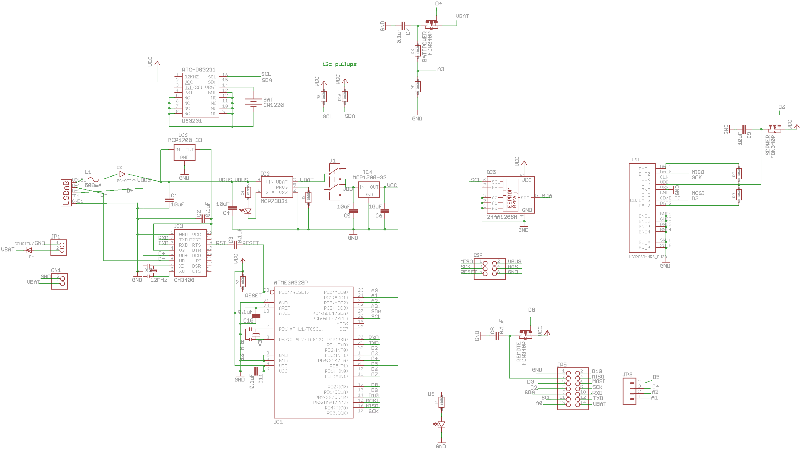
Meanwhile: Here's the latest Riffle version, 0.1.8:
https://github.com/OpenWaterProject/riffle/blob/master/hardware/riffle-beta-0.1.0/riffle-beta-0.1.8-board.png https://raw.githubusercontent.com/OpenWaterProject/riffle/master/hardware/riffle-beta-0.1.0/riffle-beta-0.1.8-schem.png
After a bunch of convos, this is the version we're thinking of locking in as a first release.
The main modifications recently have been to the power circuitry. In the end, I think we came up with a nice solution:
The switch depicted has two positions. In one position, it receives power from "VDD", which is connected to both VUSB and VBAT (the lithium battery port) via parallel diodes. This way, the device is programmable when plugged into USB but when there's no battery plugged in (power gets routed from VUSB); if you plug in both, the battery gets charged.
In the other position, the device receives power from "VGEN1". This line is connected to two power terminals. The first, CN1, is a JST connector. We didn't place a diode on this line (no danger of plugging in a JST connector "backwards", given the polar design of the connector) -- so any battery on this line goes directly into the LDO. The second, JP1, is simply two "+/-" breakouts directly on the board. This is for users who might want to make their own particular power connector. This is protected by a diode; but we've also placed a solder jumper on the back of the board that allows advanced users to bypass this diode.
I think this gives us a pretty good solution. For general prototyping and programming, one of the battery ports (CN1) is more appropriate. For really long term deployments where you want to squeeze every last drop of energy from the battery, the other battery ports (CN2 or JP1) probably work best.
For this version, we decided not to allow for routing around the LDO. We're going to reserve that feature for a possible update later. For most purposes, the LDO's quiescent power draw (1 uA for the MPC1700) shouldn't be an issue.
Further changes:
Please send any feedback or anything you notice re: errors -- but it looks like we're close to ready for a first release (exciting)!
Cheers, Don
Reply to this comment...
Log in to comment
Login to comment.