Background:We are working to develop hardware and software for low cost
visible and uv spectroscopy. Design evolution of the WheeTrometer spectrometer has been described in several PublicLab research notes. Our current design makes use of commercial optics mounted in 3d printed body and optical mounts. A video demonstrating assembly of the spectrometer is here: A video showing how to calibrate the instrument is here:
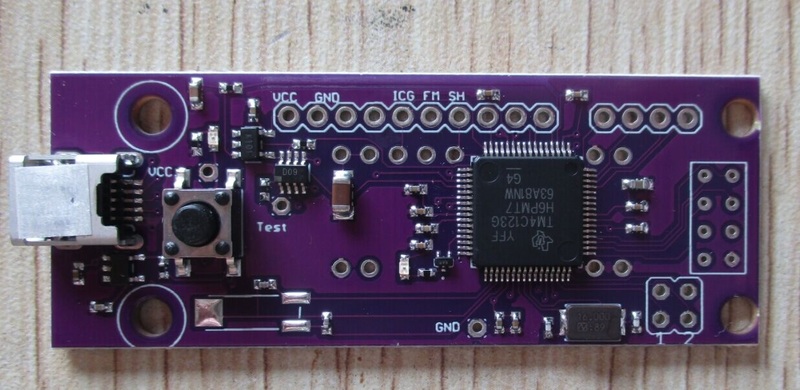
Another video shows a home built uv-vis light source and demonstrates some of the software. At the heart of our prototyping effort is our work to develop electronics for detecting light with wavelengths in the range of 200 to 1000 nm. The photo below shows a prototype circuit board based on the Toshiba tcd1403 charge coupled device (CCD) and the Texas Instruments TM4C123 microcontroller (u-controller). The CCD outputs an analog voltage which must be read by an analog to digital converter (ADC). While this prototype works well, the intensity resolution is limited by the 12 bit ADC built into the u-controller. At this time, we are prepared to sell the electronics and optics for the 12 bit resolution instrument through our website, SmokyMtSci.com. We hope to get our act together to sell the uv-vis light source some time in 2021. If you are interested in helping with the light source prototyping effort, contact me and we can discuss selling you components for the light source.

While 12 bits (~4,000 steps of resolution) is sufficient for many applications*, most commercial spectrometers use 16 bit ADCs (64,000 steps). This report documents our investigations of using an external 24 bit ADC chip, which has a theoretical resolution of ~16 million steps.
*note- In my opinion, 12 bits is plenty of resolution for a visible spectrometer. If you want to teach spectroscopy and keep the budget down, a 12 bit instrument with a tungsten-halogen light source may be the way to go. I think the higher resolution becomes more important when your light source has large variations in intensity at different wavelengths. This large variation in output is seen in the spikes seen in the spectrum of deuterium lamps which are commonly used in uv applications.
Design criteria;
One question we will eventually need to address is how much resolution is appropriate. At some point, increasing resolution will only be amplifying the noise in the measurement. It must be said that irrelevant data does not need to be reported (ie, if 16 bits is sufficient, the least significant 8 bits from a 24 bit ADC can be discarded). A second design criterion concerns the ADC maximum sampling rate. The CCD is intended to output data at a rate of 250 kHz. That means that each pixel has to be acquired and the data recorded in 4 microseconds. Our third design criterion was to make the ADC prototyping boards compatible with our existing spectrometer electronic hardware. When we designed the existing spectrometer board (figure above), we broke out a number of pins that can be used for the ADC. These including pwm, GPIO, and SPI pins. The main (title) figure for this research note shows our current prototype for the ADC board. Notice that there is a wire pad near the usb port labeled "Test" that connects to the CCD output. For the external ADC, we will remove a resistor linking this wire to the internal ADC and run a wire to the breakout board.
We decided to work with the Texas Instruments ADS127LO1 24 bit ADC. This ADC has a 512 kHz maximum sampling rate and communicates with the u-controller using SPI. The title photo for this research note shows our current breakout board prototype developed for this ADC. SPI, clock and control inputs for the ADC board are positioned to connect through headers with the appropriate pins on the u-controller board. The ADC measures voltages input at the wire pad on the left of this figure labeled "IN".
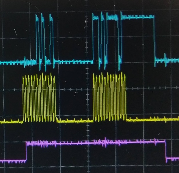
Signal timing for the ADC is pretty tight for the microcontroller we use, so a few notes on timing are appropriate. The ADC requires a variety of signals from the microcontroller. A master clock, two SPI signals (chip select and SPI clock) and a few control signals that can be tied either high or low. We recommend tying the start pin HIGH and using a GPIO pin to reset the ADC using the RESET pin. The ADC reads a voltage every 32 cycles of the master clock, so reading at 250 kHz requires an 8 MHz master clock. It also requires that all signaling be complete in 4 microseconds. In addition to these inputs, the ADC outputs signals on the MISO pin and a digital ready (DRDY) pin. The ADC drives the DRDY pin low to indicate that the read voltage has been converted to a digital signal and can be output to the microcontroller. We trigger an ADC read using an interrupt on the DRDY pin. Oscilloscope traces for the communications are presented below. The purple line is the DRDY pin, the yellow is the SPI clock and the blue is the MISO pin. Not explicitly shown in the figure is the delay between when the DRDY pin goes low and the u-controller begins outputting the SCK pulses to read the data. This delay is on the order of 1.5 microseconds, leaving us with about 2.5 microseconds to read the data before another reading is made. It is critical that both 12 cycle pulses of the yellow clock trace finish before the purple trace toggles from high to low. The firmware we use will transfer words of between 4 and 16 bits, so we read the output from the MISO pin as two 12 bit words. As shown in the photo, there is a significant delay between the two sets of SCK pulses. Vertical divisions are 0.5 microseconds apart.

Performance:
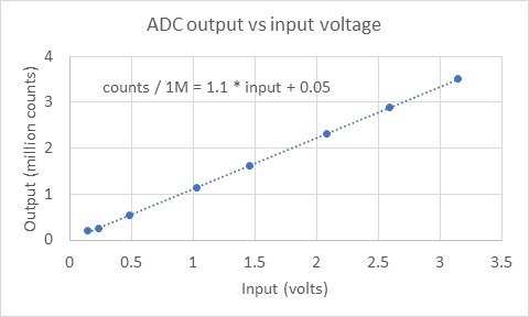
To test the ADC board, we controlled voltage at the input pin using a rotary potentiometer with the input limited to between ground
and 3.3 volts. This allowed us to vary the voltage
applied to the ADC and we monitored the digital output as a function of input voltage. A plot of digital output versus measured input voltage
is presented in the graph below.
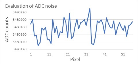
Evaluation of noise inherent to our ADC board. To evaluate noise, we grabbed 56 data points from a serial stream and plotted the output versus pixel number. The result, shown in the figure below shows that the standard deviation was 22.8 counts out of an average of more than 3 million. This means that noise from this ADC board was contained in the least significant five or six bits, leaving 18 or 19 bits of real data. That does not mean that data from the spectrometer will be good to this level; noise from the CCD is not factored in and may turn out to be the limiting factor. We also note that the noise in this board may be primarily due to electronic noise which could be improved by improvements in electronic isolation.
Conclusion
After a fairly frustrating summer, this work is turning out pretty well. While we have not tested the ADC board reading the CCD yet, our bench tests show that the ADC gives reliable, linear, high resolution, low noise data and we are confident that this approach will allow us to improve the resolution of our spectrometer.
We hope that others will find our experience useful and will build on it to make their own electronic instruments for high resolution measurements. Feel free to contact me if you want more information (schematics, design tips, code, etc). Please be aware that firmware for this project was written in Code Composer Studio, a C based IDE, and I will not be much help if you want to convert it for Arduino.


0 Comments
Login to comment.